
你继续献丑吧。懒得教育你这样的文盲
麒麟9000s的電鏡掃描結果出來了, 超過了台積電N7!
版主: Softfist
Re: 麒麟9000s的電鏡掃描結果出來了, 超過了台積電N7!
司马光在《资治通鉴》中说日本人:'知小礼而无大义,拘小节而无大德。重末节而无廉耻,畏威而不怀德。强必盗寇,弱必卑伏'。
康熙皇帝在《康熙朝起居注》中这样评论日本人:“倭子国,最是反复无常之国。其人,甚卑贱,不知世上有恩谊,只一味慑于武威……故尔,不得对其有稍许好颜色。”
康熙皇帝在《康熙朝起居注》中这样评论日本人:“倭子国,最是反复无常之国。其人,甚卑贱,不知世上有恩谊,只一味慑于武威……故尔,不得对其有稍许好颜色。”
-
fangkuuaih
- 论坛元老

- 帖子互动: 1054
- 帖子: 22668
- 注册时间: 2022年 7月 22日 09:19


Re: 麒麟9000s的電鏡掃描結果出來了, 超過了台積電N7!
台積電N7製程電晶體密度是91.2 MTr/mm²
7纳米制程DUV, EUV都可以做。
In terms of raw cell-level density, the 7-nanometer node features silicon densities between 90-102 million transistors per square millimeter based on WikiChip's own analysis.
Overview
First introduced by the major foundries around the 2018-19 timeframe, the 7-nanometer process technology is characterized by its use of FinFET transistors with fin pitches in the 30s of nanometer and densest metal pitches in the upper 30s or low 50s of nanometers. Due to the small feature sizes, quad patterning had to be utilized for some layers. This process was introduced just as EUV Lithography became ready for mass production, therefore some foundries utilized EUV while others didn't.
上次由 StMichael 在 2023年 9月 9日 20:36 修改。
Re: 麒麟9000s的電鏡掃描結果出來了, 超過了台積電N7!
所以你没有受过教育的1450就知道这么多了
司马光在《资治通鉴》中说日本人:'知小礼而无大义,拘小节而无大德。重末节而无廉耻,畏威而不怀德。强必盗寇,弱必卑伏'。
康熙皇帝在《康熙朝起居注》中这样评论日本人:“倭子国,最是反复无常之国。其人,甚卑贱,不知世上有恩谊,只一味慑于武威……故尔,不得对其有稍许好颜色。”
康熙皇帝在《康熙朝起居注》中这样评论日本人:“倭子国,最是反复无常之国。其人,甚卑贱,不知世上有恩谊,只一味慑于武威……故尔,不得对其有稍许好颜色。”
-
fangkuuaih
- 论坛元老
- 帖子互动: 1054
- 帖子: 22668
- 注册时间: 2022年 7月 22日 09:19

-
fangkuuaih
- 论坛元老
- 帖子互动: 1054
- 帖子: 22668
- 注册时间: 2022年 7月 22日 09:19
-
fangkuuaih
- 论坛元老
- 帖子互动: 1054
- 帖子: 22668
- 注册时间: 2022年 7月 22日 09:19
-
whatsupandrew
- 著名写手

- 帖子互动: 2
- 帖子: 264
- 注册时间: 2023年 1月 17日 09:49

Re: 麒麟9000s的電鏡掃描結果出來了, 超過了台積電N7!
這個單管的特徵尺寸數據基于台積電N10(66/44)和N7duv(54/40)之間
但是通過協同優化實現了6t庫和sdp技術,從而把整體密度拉到了100Mtr左右,超過了台積電N7。使得晶體管密度在N7P和N6之間。”
尼玛,写的这么清楚,。都他妈的看不懂?
但是通過協同優化實現了6t庫和sdp技術,從而把整體密度拉到了100Mtr左右,超過了台積電N7。使得晶體管密度在N7P和N6之間。”
尼玛,写的这么清楚,。都他妈的看不懂?
-
fangkuuaih
- 论坛元老
- 帖子互动: 1054
- 帖子: 22668
- 注册时间: 2022年 7月 22日 09:19
Re: 麒麟9000s的電鏡掃描結果出來了, 超過了台積電N7!
谁知道你他妈这段话哪里来的。oldmo 写了: 2023年 9月 9日 20:45 這個單管的特徵尺寸數據基于台積電N10(66/44)和N7duv(54/40)之間
但是通過協同優化實現了6t庫和sdp技術,從而把整體密度拉到了100Mtr左右,超過了台積電N7。使得晶體管密度在N7P和N6之間。”
尼玛,写的这么清楚,。都他妈的看不懂?
你翻译一下就好。

Re: 麒麟9000s的電鏡掃描結果出來了, 超過了台積電N7!
你懂个p
中国电能产能世界第一
这点漏电量 三峡大坝手指缝儿里漏出来一点点 就够全国芯片漏的电用了
1450殖人轮逼语录系列:
叔的凤凰卫视高层朋友告诉我 只要菊花一晚 就能告诉我秦刚内幕
- 纯属虚构 如有雷同 必为巧合 切勿对号入座
VladPutin是我爹 我以我爹赐名为荣
- 某买买提轮逼精神白人 / 切勿对号入座
洋人有特权,白妞特权还高一些。这要是黄妞,早被当地公安跨省了
中国不敢公布 所以证明中国基尼系数越来越高
- 某轮逼1450反串网友WxxxxMxxxSxxxJxxx
叔的凤凰卫视高层朋友告诉我 只要菊花一晚 就能告诉我秦刚内幕
- 纯属虚构 如有雷同 必为巧合 切勿对号入座
VladPutin是我爹 我以我爹赐名为荣
- 某买买提轮逼精神白人 / 切勿对号入座
洋人有特权,白妞特权还高一些。这要是黄妞,早被当地公安跨省了
中国不敢公布 所以证明中国基尼系数越来越高
- 某轮逼1450反串网友WxxxxMxxxSxxxJxxx

-
fangkuuaih
- 论坛元老
- 帖子互动: 1054
- 帖子: 22668
- 注册时间: 2022年 7月 22日 09:19
Re: 麒麟9000s的電鏡掃描結果出來了, 超過了台積電N7!

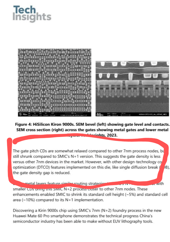
跟据techinsight的电镜图,算单个cell的size, 算出半导体密度
但看pitch工艺没意义。
别家7nm用 EUV做, pitch 更窄也不稀奇。预料之中。但是经过别的优化,实现了超越台积电7纳米半导体密度
“cpp(Contact Poly Pitch)63nm,mpp(Min Metal Pitch)40nm,高密度库6track
std cell面积 = cpp×mmp×6
这个单管的特征尺寸数据基于台积电N10(66/44)和N7 duv(54/40)之间
但是通过与某司的协同优化实现了6t库和sdp技术,从而把整体密度拉到了100Mtr左右,超过了台积电N7。使得晶体管密度在N7P和N6之间